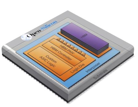
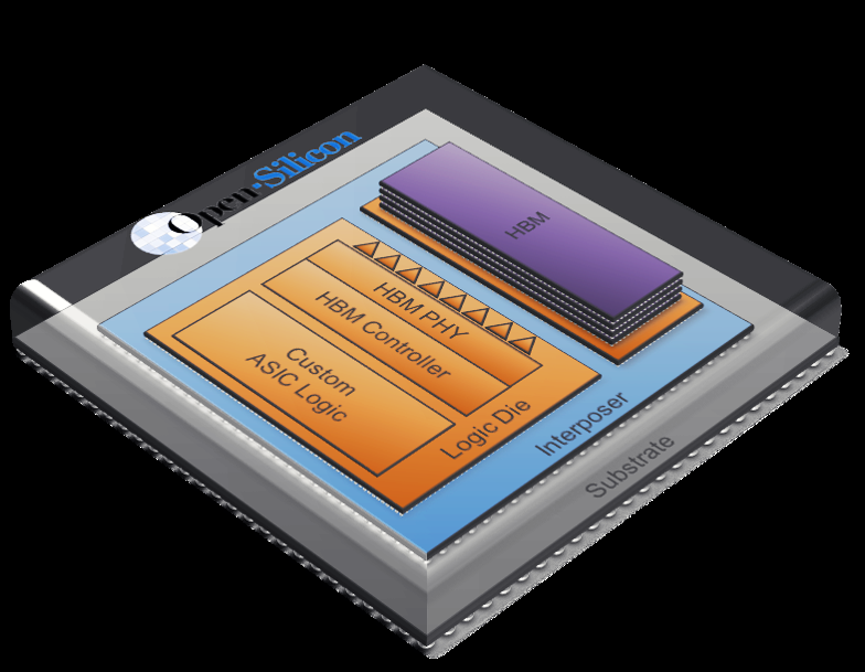
Open-Silicon Tapes Out Industry's First High Bandwidth Memory

Accelerating High-Bandwidth Memory to light speed – Blocks and Files

Advanced Packaging Technologies Overcoming the Memory System Performance and Capacity Limitation - EE Times

Closing the Memory Gap: Can Advanced Fab and Packaging Finally
🔮E14: The Real AI Bottleneck: High Bandwidth Memory (HBM)

Closing The Performance Gap Between DRAM And AI Processors
Open-Silicon Announces Comprehensive High Bandwidth Memory (HBM) Gen2 IP Subsystem Solution
Alphawave Semi Spearheads Chiplet-Based Custom Silicon for Generative AI and Data Center Workloads with Successful 3nm Tapeouts of HBM3 and UCIe IP
Samsung Begins Mass Producing World's Fastest DRAM – Based on Newest High Bandwidth Memory (HBM) Interface – Samsung Global Newsroom

Deep Etching of Single- and Polycrystalline Silicon with High Speed, High Aspect Ratio, High Uniformity, and 3D Complexity by Electric Bias-Attenuated Metal-Assisted Chemical Etching (EMaCE)
Open-Silicon Tapes Out Industry's First High Bandwidth Memory (HBM2) IP Subsystem Solution for 2.5D ASICs in 16nm FF+
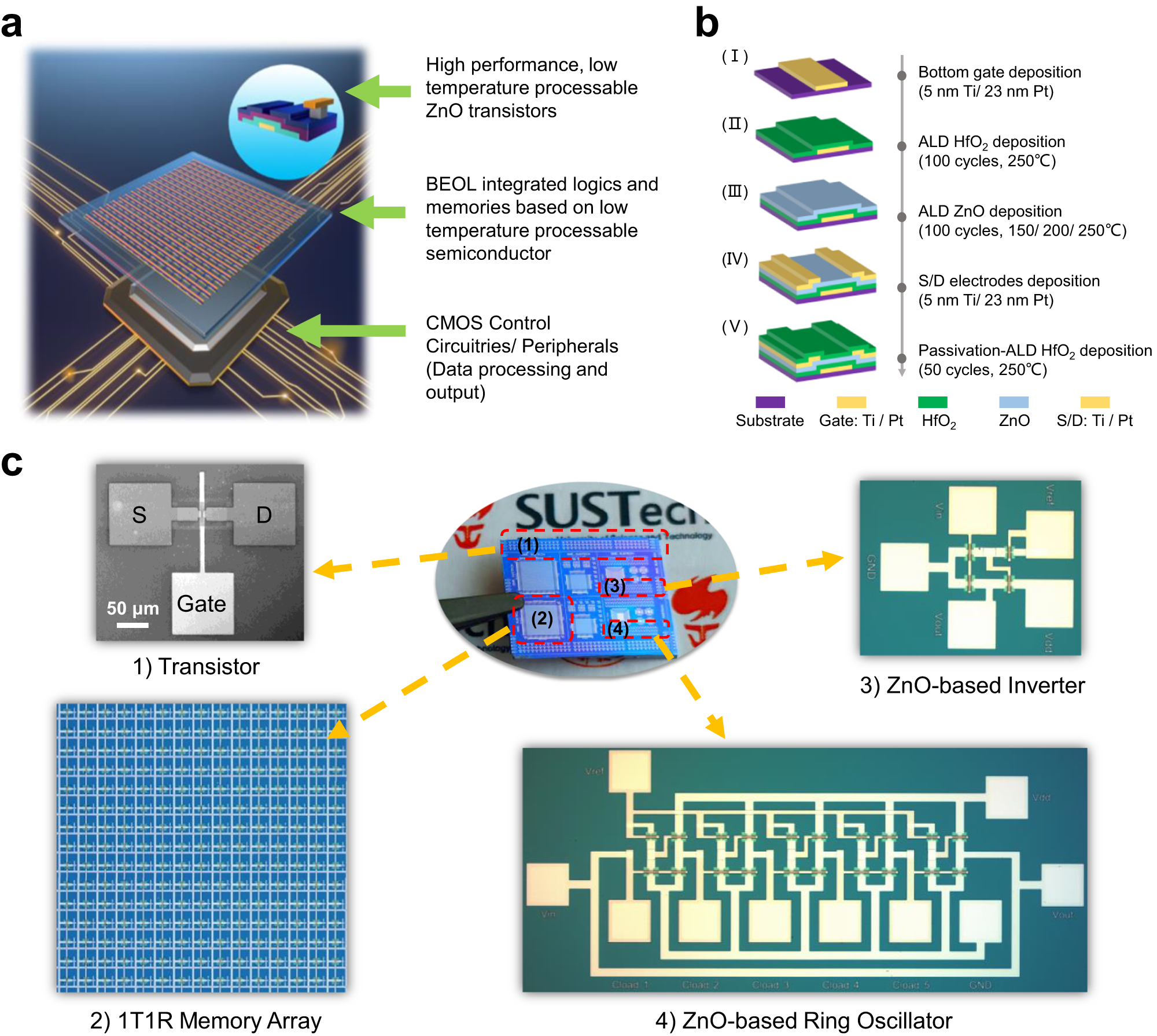
CMOS backend-of-line compatible memory array and logic circuitries enabled by high performance atomic layer deposited ZnO thin-film transistor