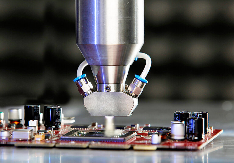
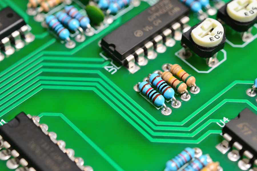
Why Plasma Activation of PCBs Ensures Conformal Coating Results
Plasma activation of PCBs with a plasma cleaning step are excellent processes include in any printed circuit board manufacturing line. Learn why.
Electronics Plasmatreat

Opportunities of Electronic and Optical Sensors in Autonomous Medical Plasma Technologies
The Conformal Coating Process for PCBAs, Advanced PCB Design Blog

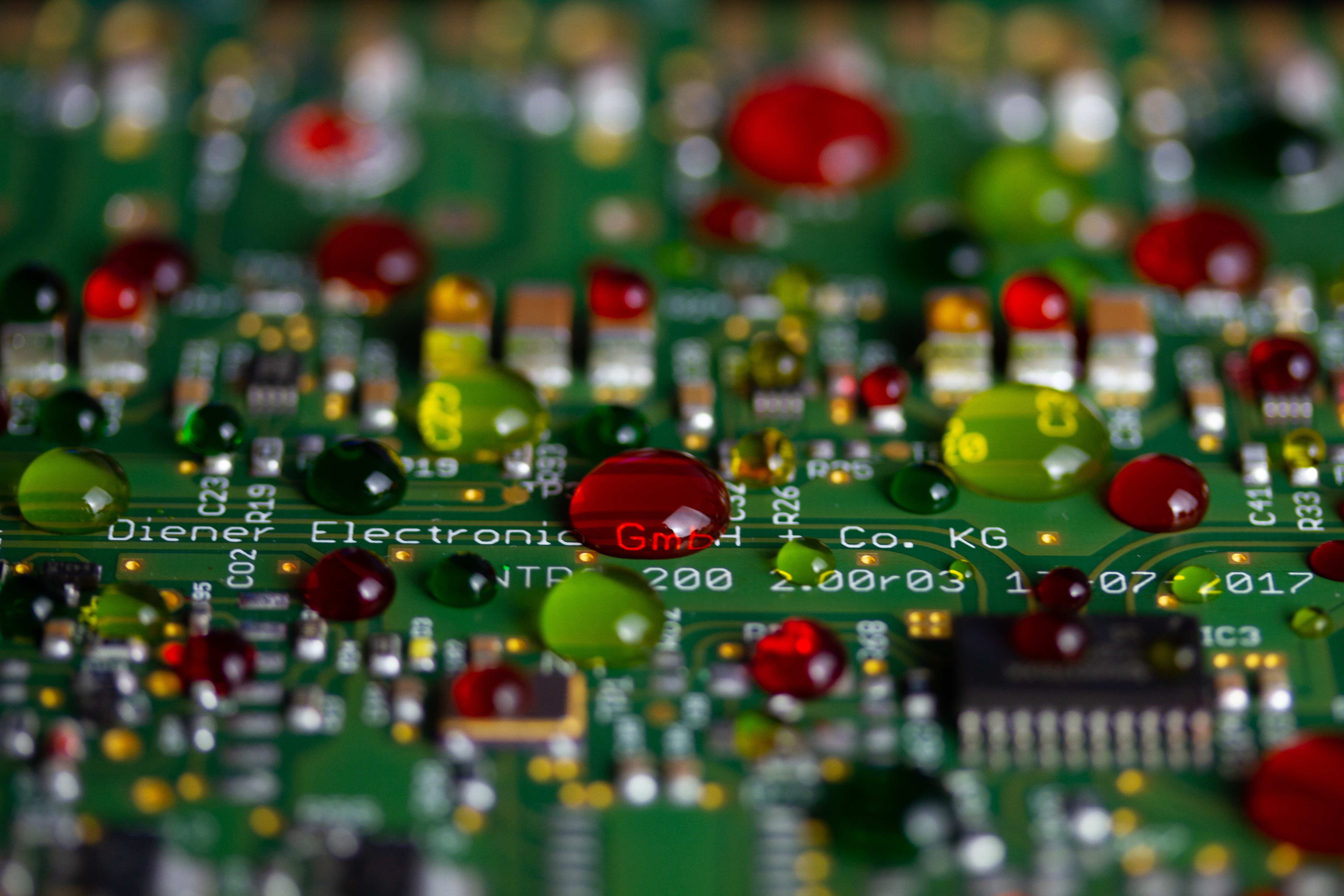
Seal the Deal with Conformal Coating
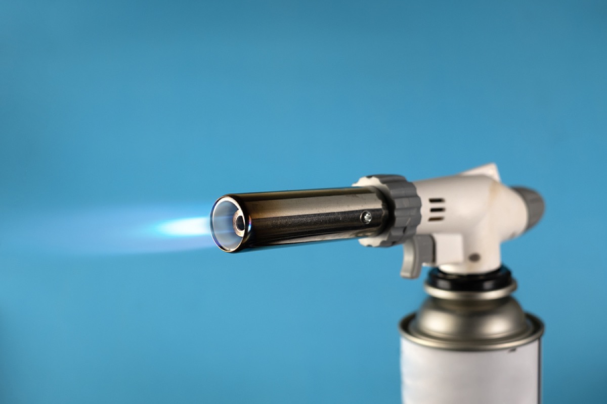
The Dirty Secret of Flame Treatment in Manufacturing
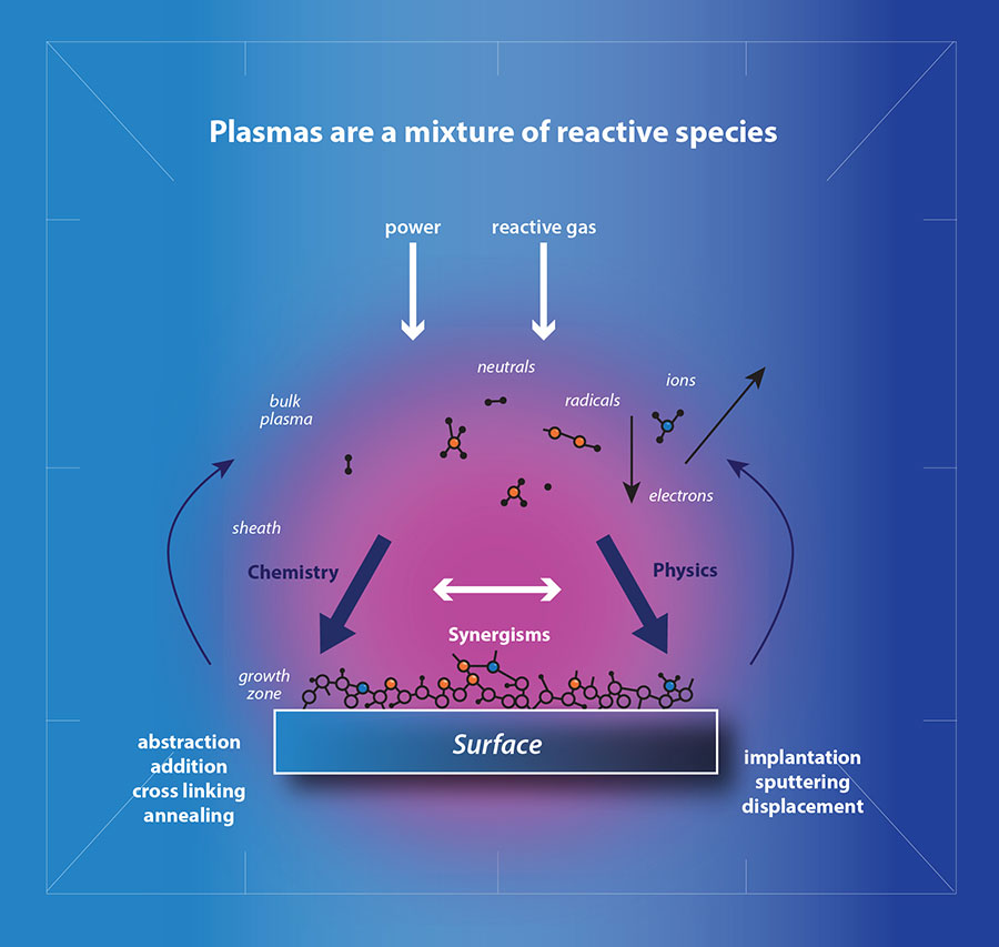
Plasma Treatment Explained in Simple Terms - Henniker Plasma

Demand for plasma applications prior to conformal coating process

How the Functionality of Electronic Devices is Affected by the Conformal Coating Thickness on PCB - RAYPCB
Sensors, Free Full-Text
Plasma Cleaning in the Electronics Industry - Henniker Plasma

Laser Direct Activation of Polyimide for Selective Electroless Plating of Flexible Conductive Patterns
Frontiers Influence of Air Plasma Pretreatments on Mechanical Properties in Metal-Reinforced Laminated Wood
Why Plasma Activation of PCBs Ensures Conformal Coating Results
Why Plasma Activation of PCBs Ensures Conformal Coating Results