What is the Electrical Return Path in a PCB?
One of the fundamental aspects of any circuit diagram is the return current path or electrical return path. In a circuit diagram and a schematic diagram, the path the current follows to return to the low potential side of a power source should be obvious, but it may not be so obvious in a PCB.

The Path of Least Impedance: How to Use Return Paths for Better PCB Design - Technical Articles

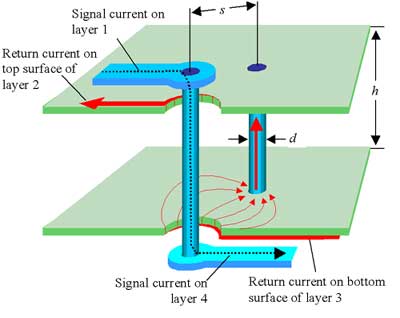
Signal Current Path and Return Current Path of 4-layer PCB. Return
Signal Current Path and Return Current Path of 4-layer PCB. Return

Return Path - an overview
The Plane Facts of PCB Return Current Paths, Advanced PCB Design Blog

What Every PCB Designer Should Know - Return Current Path (with Eric Bogatin)

How to Handle Current Return Path for Better Signal Integrity
8 PCB Grounding Rules to Live By, EAGLE
Layout guidelines for good Return Path in PCB – RAM SYSTEMS

Return Path Design Rule

pcb design - Where does the power supply current return? - Electrical Engineering Stack Exchange

Return Current - What is Return Current in a PCB?

The high-speed PCB signal return and cross- segmentation - Engineering Technical - PCBway

How to Design Your PCB Return Current Path

Step-by-Step Example for Practical PCB Design - Power Supply Design Tutorial Section 3-3 - Power Electronics News